- 您现在的位置:买卖IC网 > Sheet目录890 > XCL209F083DR (Torex Semiconductor Ltd)IC STEP DOWN DC/DC 0.8V USP10B03
�� �
�
�XCL208/XCL209�
�Series�
�■� NOTE� ON� USE�
�1.� For� temporary,� transitional� voltage� drop� or� voltage� rising� phenomenon,� the� IC� is� liable� to� malfunction� should� the� ratings� be�
�exceeded.�
�2.� The� XCL208/XCL209� series� is� designed� for� use� with� ceramic� output� capacitors.� If,� however,� the� potential� difference� is� too�
�large� between� the� input� voltage� and� the� output� voltage,� a� ceramic� capacitor� may� fail� to� absorb� the� resulting� high� switching�
�energy� and� oscillation� could� occur� on� the� output.� In� this� case,� increase� 10� μ� F� to� the� output� capacitance� for� adding�
�insufficient� capacitance.� Also,� if� the� output� capacitance� is� too� large,� the� output� voltage� is� slowly� rising� and� the� IC� may� not�
�operate.� Adjust� the� output� capacitance� so� that� the� output� voltage� can� go� up� within� the� soft-start� time.�
�3.� Spike� noise� and� ripple� voltage� arise� in� a� switching� regulator� as� with� a� DC/DC� converter.� These� are� greatly� influenced� by�
�external� component� selection,� such� as� the� coil� inductance,� capacitance� values,� and� board� layout� of� external� components.�
�Once� the� design� has� been� completed,� verification� with� actual� components� should� be� done.�
�4.� Depending� on� the� input-output� voltage� differential,� or� load� current,� some� pulses� may� be� skipped� as� 1/2,� 1/3� and� the� ripple� voltage�
�may� increase.�
�5.� When� the� difference� between� input� and� output� is� large� in� PWM� control,� very� narrow� pulses� will� be� outputted,� and� there� is� the�
�possibility� that� 0%� duty� cycles� may� be� continued� during� some� cycles.�
�6.� When� the� difference� between� input� and� output� is� small,� and� the� load� current� is� heavy,� very� wide� pulses� will� be� outputted� and�
�there� is� the� possibility� that� 100%� duty� cycles� may� be� continued� during� some� cycles.�
�7.� With� the� IC,� the� peak� current� of� the� coil� is� controlled� by� the� current� limit� circuit.� Since� the� peak� current� of� the� coil� increases�
�when� dropout� voltage� or� load� current� is� high,� current� limit� starts� operation,� and� this� can� lead� to� instability.� When� peak� current�
�becomes� high,� please� adjust� the� coil� inductance� value� and� fully� check� the� circuit� operation.� In� addition,� please� calculate� the�
�peak� current� according� to� the� following� formula:�
�Ipk� =� (V� IN� -� V� OUT� )� x� OnDuty� /� (2� x� L� x� f� OSC� )� +� I� OUT�
�L:� Coil� Inductance� Value�
�f� OSC� :� Oscillation� Frequency�
�8.� When� the� peak� current� which� exceeds� limit� current� flows� within� the� specified� time,� the� built-in� P-ch� driver� transistor� turns� off.�
�During� the� time� until� it� detects� limit� current� and� before� the� built-in� transistor� can� be� turned� off,� the� current� for� limit� current�
�flows;� therefore,� care� must� be� taken� when� selecting� the� rating� for� the� external� components� such� as� a� coil.�
�9.� When� V� IN� is� less� than� 2.4V,� limit� current� may� not� be� reached� because� voltage� falls� caused� by� ON� resistance.�
�10.� Depending� on� the� state� of� the� PC� Board,� latch� time� may� become� longer� and� latch� operation� may� not� work.� In� order� to� avoid�
�the� effect� of� noise,� the� board� should� be� laid� out� so� that� input� capacitors� are� placed� as� close� to� the� IC� as� possible.�
�11.� Use� of� the� IC� at� voltages� below� the� minimum� operating� voltage� range� may� lead� to� instability.�
�12.� This� IC� should� be� used� within� the� stated� absolute� maximum� ratings� of� external� components� in� order� to� prevent� damage� to�
�the� device.�
�13.� When� the� IC� is� used� in� high� temperature,� output� voltage� may� increase� up� to� input� voltage� level� at� no� load� because� of� the�
�leak� current� of� the� driver� transistor.�
�14.� The� current� limit� is� set� to� 1000mA� (MAX.)� at� typical.� However,� the� current� of� 1000mA� or� more� may� flow.�
�In� case� that� the� current� limit� functions� while� the� V� OUT� pin� is� shorted� to� the� GND� pin,� when� P-ch� MOSFET� is� ON,� the� potential�
�difference� for� input� voltage� will� occur� at� both� ends� of� a� coil.� For� this,� the� time� rate� of� coil� current� becomes� large.� By�
�contrast,� when� N-ch� MOSFET� is� ON,� there� is� almost� no� potential� difference� at� both� ends� of� the� coil� since� the� V� OUT� pin� is�
�shorted� to� the� GND� pin.� Consequently,� the� time� rate� of� coil� current� becomes� quite� small.� According� to� the� repetition� of� this�
�operation,� and� the� delay� time� of� the� circuit,� coil� current� will� be� converged� on� a� certain� current� value,� exceeding� the� amount� of�
�current,� which� is� supposed� to� be� limited� originally.� Even� in� this� case,� however,� after� the� over� current� state� continues� for�
�several� ms,� the� circuit� will� be� latched.� A� coil� should� be� used� within� the� stated� absolute� maximum� rating� in� order� to� prevent�
�damage� to� the� device.�
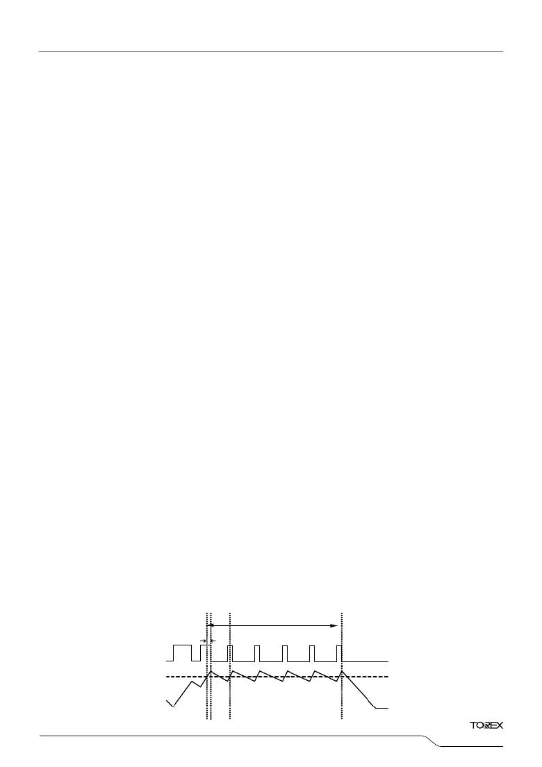
�①� Current� flows� into� P-ch� MOSFET� to� reach� the� current� limit� (I� LIM� ).�
�②� The� current� of� I� LIM� or� more� flows� since� the� delay� time� of� the� circuit� occurs� during� from� the� detection� of� the� current� limit� to� OFF� of� P-ch� MOSFET.�
�③� Because� of� no� potential� difference� at� both� ends� of� the� coil,� the� time� rate� of� coil� current� becomes� quite� small.�
�④� Lx� oscillates� very� narrow� pulses� by� the� current� limit� for� several� ms.�
�⑤� The� circuit� is� latched,� stopping� its� operation.�
�②�
�①�
�Delay�
�③�
�④�
�Limit� >� #ms�
�⑤�
�Lx�
�I� LIM�
�I� Lx�
�13/22�
�发布紧急采购,3分钟左右您将得到回复。
相关PDF资料
XHB-00
POWER CHASSIS 600W 6 SLOT
XKC-00
POWER CHASSIS 600W 4 SLOT
XMD-01
POWER CHASSIS 750W 4 SLOT
XNB-01
POWER CHASSIS 400W 4 SLOT
XQC-00
POWER CHASSIS 1200W 6 SLOT
XRC-00
POWER CHASSIS 600W 4 SLOT
XTB-01
POWER CHASSIS 400W 4 SLOT
XVD-01
POWER CHASSIS 1200W 6 SLOT
相关代理商/技术参数
XCL209F083DR-G
制造商:Torex Semiconductor LTD 功能描述:IC STEP DOWN DC/DC 0.8V USP10B03
XCL210C101GR-G
功能描述:200MA INDUCTOR BUILT-IN PFM STEP 制造商:torex semiconductor ltd 系列:XCL210 包装:剪切带(CT) 零件状态:有效 类型:非隔离 PoL 模块 输出数:1 电压 - 输入(最小值):2V 电压 - 输入(最大值):6V 电压 - 输出 1:1V 电压 - 输出 2:- 电压 - 输出 3:- 电流 - 输出(最大值):200mA 功率(W) - 制造系列:- 电压 - 隔离:- 应用:ITE(商业) 特性:SCP,UVLO 安装类型:表面贴装 封装/外壳:8-SMD 大小/尺寸:0.10" 长 x 0.08" 宽 x 0.04" 高(2.5mm x 2.0mm x 1.04mm) 工作温度:-40°C ~ 85°C 效率:93% 功率(W) - 最大值:- 标准包装:1
XCL210C121GR-G
功能描述:200MA INDUCTOR BUILT-IN PFM STEP 制造商:torex semiconductor ltd 系列:XCL210 包装:剪切带(CT) 零件状态:有效 类型:非隔离 PoL 模块 输出数:1 电压 - 输入(最小值):2V 电压 - 输入(最大值):6V 电压 - 输出 1:1.2V 电压 - 输出 2:- 电压 - 输出 3:- 电流 - 输出(最大值):200mA 功率(W) - 制造系列:- 电压 - 隔离:- 应用:ITE(商业) 特性:SCP,UVLO 安装类型:表面贴装 封装/外壳:8-SMD 大小/尺寸:0.10" 长 x 0.08" 宽 x 0.04" 高(2.5mm x 2.0mm x 1.04mm) 工作温度:-40°C ~ 85°C 效率:93% 功率(W) - 最大值:- 标准包装:1
XCL210C151GR-G
功能描述:200MA INDUCTOR BUILT-IN PFM STEP 制造商:torex semiconductor ltd 系列:XCL210 包装:剪切带(CT) 零件状态:有效 类型:非隔离 PoL 模块 输出数:1 电压 - 输入(最小值):2V 电压 - 输入(最大值):6V 电压 - 输出 1:1.5V 电压 - 输出 2:- 电压 - 输出 3:- 电流 - 输出(最大值):200mA 功率(W) - 制造系列:- 电压 - 隔离:- 应用:ITE(商业) 特性:SCP,UVLO 安装类型:表面贴装 封装/外壳:8-SMD 大小/尺寸:0.10" 长 x 0.08" 宽 x 0.04" 高(2.5mm x 2.0mm x 1.04mm) 工作温度:-40°C ~ 85°C 效率:93% 功率(W) - 最大值:- 标准包装:1
XCL210C181GR-G
功能描述:200MA INDUCTOR BUILT-IN PFM STEP 制造商:torex semiconductor ltd 系列:XCL210 包装:剪切带(CT) 零件状态:有效 类型:非隔离 PoL 模块 输出数:1 电压 - 输入(最小值):2V 电压 - 输入(最大值):6V 电压 - 输出 1:1.8V 电压 - 输出 2:- 电压 - 输出 3:- 电流 - 输出(最大值):200mA 功率(W) - 制造系列:- 电压 - 隔离:- 应用:ITE(商业) 特性:SCP,UVLO 安装类型:表面贴装 封装/外壳:8-SMD 大小/尺寸:0.10" 长 x 0.08" 宽 x 0.04" 高(2.5mm x 2.0mm x 1.04mm) 工作温度:-40°C ~ 85°C 效率:93% 功率(W) - 最大值:- 标准包装:1
XCL210C251GR-G
功能描述:200MA INDUCTOR BUILT-IN PFM STEP 制造商:torex semiconductor ltd 系列:XCL210 包装:剪切带(CT) 零件状态:有效 类型:非隔离 PoL 模块 输出数:1 电压 - 输入(最小值):2V 电压 - 输入(最大值):6V 电压 - 输出 1:2.5V 电压 - 输出 2:- 电压 - 输出 3:- 电流 - 输出(最大值):200mA 功率(W) - 制造系列:- 电压 - 隔离:- 应用:ITE(商业) 特性:SCP,UVLO 安装类型:表面贴装 封装/外壳:8-SMD 大小/尺寸:0.10" 长 x 0.08" 宽 x 0.04" 高(2.5mm x 2.0mm x 1.04mm) 工作温度:-40°C ~ 85°C 效率:93% 功率(W) - 最大值:- 标准包装:1
XCL210C281GR-G
功能描述:200MA INDUCTOR BUILT-IN PFM STEP 制造商:torex semiconductor ltd 系列:XCL210 包装:剪切带(CT) 零件状态:有效 类型:非隔离 PoL 模块 输出数:1 电压 - 输入(最小值):2V 电压 - 输入(最大值):6V 电压 - 输出 1:2.8V 电压 - 输出 2:- 电压 - 输出 3:- 电流 - 输出(最大值):200mA 功率(W) - 制造系列:- 电压 - 隔离:- 应用:ITE(商业) 特性:SCP,UVLO 安装类型:表面贴装 封装/外壳:8-SMD 大小/尺寸:0.10" 长 x 0.08" 宽 x 0.04" 高(2.5mm x 2.0mm x 1.04mm) 工作温度:-40°C ~ 85°C 效率:93% 功率(W) - 最大值:- 标准包装:1
XCL210C301GR-G
功能描述:200MA INDUCTOR BUILT-IN PFM STEP 制造商:torex semiconductor ltd 系列:XCL210 包装:剪切带(CT) 零件状态:有效 类型:非隔离 PoL 模块 输出数:1 电压 - 输入(最小值):2V 电压 - 输入(最大值):6V 电压 - 输出 1:3V 电压 - 输出 2:- 电压 - 输出 3:- 电流 - 输出(最大值):200mA 功率(W) - 制造系列:- 电压 - 隔离:- 应用:ITE(商业) 特性:SCP,UVLO 安装类型:表面贴装 封装/外壳:8-SMD 大小/尺寸:0.10" 长 x 0.08" 宽 x 0.04" 高(2.5mm x 2.0mm x 1.04mm) 工作温度:-40°C ~ 85°C 效率:93% 功率(W) - 最大值:- 标准包装:1